EU6865Q1
- Description
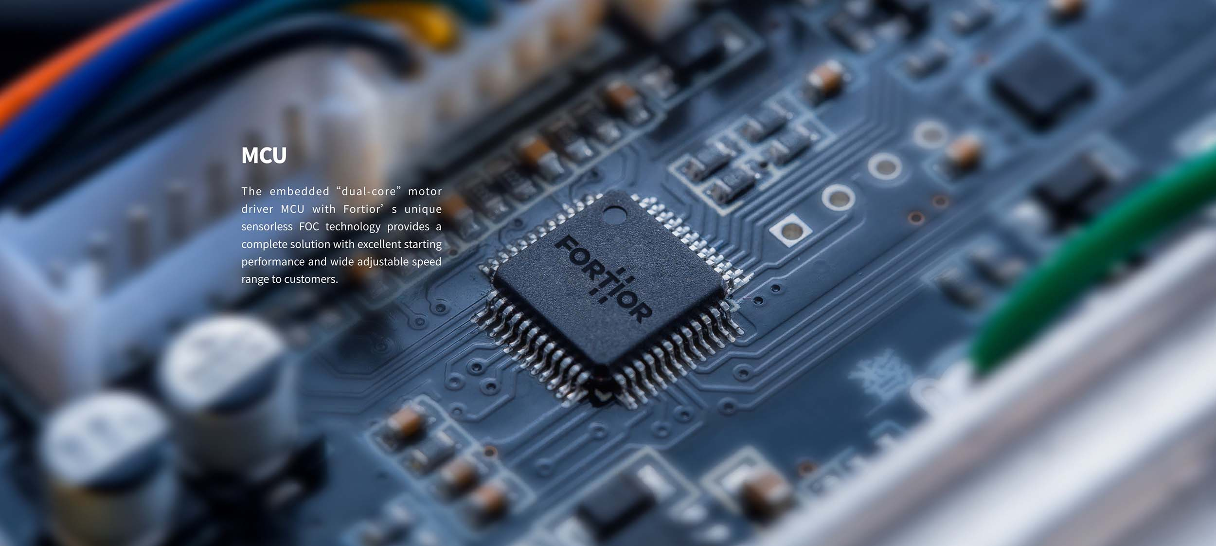
- The high-performance motor drive chip incorporates ME core and 8051 core. ME core integrates FOC,
MDU, LPF, PID and SVPWM modules that allow for automatic calculation of FOC or square-wave control
by the hardware for sensored/sensorless BLDC motors. 8051 core is used for parameter configuration and
routine processing. Most of 8051 core instruction cycle takes 1T or 2T clock cycle(s). The dual cores work in
parallel to achieve high-performance motor control. The chip integrates high-speed operational amplifiers,
comparators, PWM (for EU6815Q1), pre-driver (for EU6865Q1), high-speed ADC, CRC, SPI, I2C, UART,
Timers, built-in high-voltage LDO, which are suitable for FOC or square-wave based BLDC motors.
Package type of EU6815Q1: QFN48
Package type of EU6865Q1: QFN56
- Features
-
Features
◼ Power supply:
➢ High-voltage single-power supply mode: When VCC_MODE = 0, external power supply
5V~18V is connected to VCC pin, and internal LDO supplies VDD5 voltage.
➢ Low-voltage single-power supply mode: When VCC_MODE = 1, external power supply
3V~5.5V is connected to VDD5 pin, and VDD5 pin is shorted to VCC pin.
Note: VDRV voltage of EU6865Q1 is supplied by external power supply.
◼ Dual-core: 8051 core and ME core
◼ An instruction cycle mostly takes 1 or 2 system clock cycle(s)
◼ 32kB Flash ROM with CRC, self-program and code protection
◼ 256 bytes IRAM and 3.75k bytes XRAM
◼ ME: Core integrating PID module, FOC module, MDU auxiliary computing module and LPF module
◼ 16 interrupt sources with 4 configurable priority levels
◼ GPIO:
➢ EU6815Q1: 38 GPIOs
➢ EU6865Q1: 36 GPIOs
◼ Timers:
➢ Timer1: Timer designed for square-wave motor drive, supporting square-wave drive timing control,
automatic commutation, cycle-by-cycle current limiting and Hall/BEMF-based position sensing
➢ Timer2: Timer supporting PWM output, measurement of duty cycle and period of input PWM
wave, measurement of the time of set PWM wave numbers, QEP decoding, tailwind/headwind
detection, and rotation direction and speed detection of step motor
➢ Timer3/Timer4: Timers supporting PWM output, and measurement of duty cycle and period of
input PWM wave. Timer4 supports FG generation and Timer3 supports up to 48MHz input.
➢ Systick Timer
➢ RTC
◼ Communication interfaces:
➢ 1 SPI
➢ 1 I2C
➢ 2 UARTs, supporting single-wire mode
➢ Dual-channel DMA, supporting data transmission via I2C, SPI and UART
◼ Analog peripherals:
➢ 12-bit ADC, operating with 1μs conversion time and internal VREF or external VREF selectable
as reference voltage
➢ Number of ADC channels:
◆ 14
➢ Built-in VREF, with 3V, 4V, 4.5V or VDD5 as the internal reference
➢ Built-in VHALF, with VREF/2, 1/4 VREF, 1/8 VREF or 25/64 VREF as the internal reference
➢ 4 standalone operational amplifiers, where PGA is configurable
➢ 4-channel analog comparator
➢ DAC: Single-channel 9-bit, single-channel 8-bit, single-channel 6-bit
◼ Driver type
➢ PWM output (for EU6815Q1)
➢ Built-in MOSFET driver: 6N pre-driver output (for EU6865Q1)
◼ FOC module supports single/dual/triple-shunt current sampling
◼ PFC
◼ System clock
➢ Built-in 24MHz fast RC oscillator
➢ Built-in 32.8kHz slow RC oscillator
➢ External 32768Hz crystal clock
◼ WDT
◼ LVD
◼ TSD
◼ Two-wire FICE protocol based in-circuit emulation
◼ AEC-Q100 (Grade 1)
- Package
-
QFN56
- Datasheet
-
Download